Lith Corporation, founded in 1998 by a group of material science doctor from Tsinghua University, has now become the leading manufacturer of battery lab&production equipment. Lith Corporation have production factories in shenzhen and xiamen of China.This allows for the possibility of providing high quality and low-cost precision machines for lab&production equipment,including: roller press, film coater,mixer, high-temperature furnace, glove box,and complete set of equipment for research of rechargeable battery materials. Simple to operate, low cost and commitment to our customers is our priority.
Thin Film System: Advanced Equipment for High-Precision Coating and Deposition
Overview
A Thin Film System is a specialized piece of equipment designed to deposit uniform, high-quality thin films onto a variety of substrates. These systems are essential in research, development, and industrial applications where precise control over film thickness, composition, and uniformity is required. Thin film systems operate using techniques such as physical vapor deposition (PVD), chemical vapor deposition (CVD), or hybrid approaches, enabling the creation of metallic, ceramic, organic, and composite coatings.
The versatility and precision of thin film systems make them indispensable in electronics, optics, materials science, and nanotechnology. By providing a controlled environment—often under high vacuum or controlled atmosphere—these systems minimize contamination, ensure repeatable deposition, and allow complex multilayer structures to be fabricated with high fidelity. Laboratory-scale, benchtop, and industrial thin film systems are available to accommodate research, pilot-scale experiments, or full-scale production needs.
Features
Modern thin film systems integrate a range of features designed to optimize performance, reliability, and ease of operation:
1. High-Vacuum or Controlled Environment Chamber
The vacuum or controlled atmosphere chamber reduces contamination and allows precise control over deposition conditions, critical for high-purity and uniform films.
2. Multiple Deposition Sources
Thin film systems may incorporate thermal evaporation sources, electron-beam evaporation, magnetron sputtering, or chemical precursors, allowing a wide range of materials to be deposited.
3. Substrate Holders with Motion Control
Substrates are often mounted on holders capable of rotation, tilting, or oscillation to achieve uniform deposition and coverage on complex geometries.
4. Thickness and Deposition Rate Monitoring
Quartz crystal microbalance (QCM) sensors or optical monitoring devices provide real-time measurement of film thickness and deposition rate, ensuring accurate process control.
5. Digital Control and Automation
Programmable control systems enable operators to set deposition parameters such as power, temperature, deposition rate, and timing, ensuring reproducibility and consistency across experiments or production runs.
6. Safety and Maintenance Features
Systems are designed with interlocks, temperature protections, and easy-access modular components to facilitate safe operation and simplify maintenance.
Process
The thin film deposition process depends on the chosen technique but typically involves the following steps:
1. Substrate Preparation
Substrates are cleaned and sometimes pretreated to remove surface contaminants and improve adhesion.
2. Chamber Evacuation or Environment Control
The system chamber is sealed and evacuated or filled with controlled gas to establish the necessary deposition environment.
3. Deposition
* Physical Vapor Deposition (PVD): Material is vaporized using thermal, electron-beam, or sputtering techniques and condenses onto the substrate.
* Chemical Vapor Deposition (CVD): Reactive gases form a thin film on the substrate through chemical reactions at elevated temperatures.
4. Monitoring and Adjustment
Deposition rate and film thickness are monitored in real time, and process parameters are adjusted to ensure uniformity and accuracy.
5. Completion and Post-Processing
Once the desired thickness is achieved, the system is cooled, the environment restored to ambient conditions, and coated substrates are removed. Additional post-processing may include annealing or surface treatments to enhance film properties.
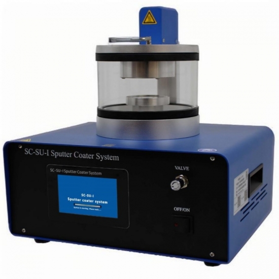
Lab PVD Sputtering System
Applications
Thin film systems have wide-ranging applications across research and industrial sectors:
* Electronics and Semiconductors: Deposition of conductive, dielectric, and protective layers for integrated circuits, sensors, and MEMS devices.
* Optics and Photonics: Fabrication of mirrors, anti-reflective coatings, optical filters, and multilayer optical devices.
* Nanotechnology and Materials Research: Creation of nanoscale coatings to study electrical, magnetic, and optical properties.
* Energy Applications: Coating of photovoltaic cells, batteries, and fuel cells with conductive or protective layers.
* Biomedical and Surface Engineering: Functional coatings for implants, bio-compatible surfaces, and thin protective layers on instruments.
Advantages
Thin film systems offer several key advantages:
1. High Purity and Quality: Controlled deposition conditions minimize contamination and produce high-integrity films.
2. Precise Thickness Control: Real-time monitoring enables accurate control of film thickness and uniformity.
3. Versatility: Supports deposition of metals, oxides, ceramics, organics, and multilayer structures.
4. Uniform Coating: Substrate motion and optimized chamber design ensure consistent coverage even on complex surfaces.
5. Scalable: Available in benchtop, laboratory, and industrial configurations to suit various research or production needs.
6. Flexible Process Control: Digital interfaces and programmable recipes enable reproducible and adjustable deposition processes.
Conclusion
Thin film systems are essential tools for producing high-quality, uniform coatings with precise control over material properties. Their versatility, precision, and reliability make them critical in electronics, optics, nanotechnology, energy devices, and biomedical applications.
By offering advanced features such as high-vacuum operation, multiple deposition sources, substrate motion, and real-time monitoring, thin film systems allow researchers and manufacturers to create complex multilayer structures and functional coatings efficiently. Whether in a laboratory, pilot-scale, or industrial production setting, thin film systems provide a reliable platform for advancing materials research, device fabrication, and surface engineering technologies.


 +86 13174506016
 Louis@lithmachine.com
 +86 18559646958
 18659217588
 English ▼


