Lith Corporation, founded in 1998 by a group of material science doctor from Tsinghua University, has now become the leading manufacturer of battery lab&production equipment. Lith Corporation have production factories in shenzhen and xiamen of China.This allows for the possibility of providing high quality and low-cost precision machines for lab&production equipment,including: roller press, film coater,mixer, high-temperature furnace, glove box,and complete set of equipment for research of rechargeable battery materials. Simple to operate, low cost and commitment to our customers is our priority.
Atomic Layer Deposition: Precision Equipment for Advanced Thin Film Fabrication
Overview
Atomic Layer Deposition (ALD) is a cutting-edge thin film deposition technology that enables the growth of highly uniform, conformal coatings at the atomic scale. ALD operates on the principle of sequential, self-limiting surface reactions, where precursor chemicals are introduced one at a time into a vacuum or controlled environment chamber. Each precursor reacts with the substrate surface in a layer-by-layer manner, allowing unparalleled control over film thickness, composition, and uniformity.
ALD systems are widely used in research laboratories, semiconductor manufacturing, optics, and nanotechnology due to their ability to create ultra-thin films with excellent conformity, even on substrates with complex geometries. Unlike conventional deposition methods, ALD provides atomic-level precision, making it indispensable for modern device fabrication where uniformity, reliability, and reproducibility are critical.
Features
Modern ALD systems incorporate a range of features designed to optimize process control, film quality, and operational safety:
1. High-Vacuum or Controlled Atmosphere Chamber
ALD chambers maintain low pressures or controlled gas atmospheres to minimize contamination and ensure precise precursor delivery.
2. Precursor Delivery and Pulse Control
Sophisticated precursor delivery systems control the timing, flow, and dosage of chemical precursors to achieve self-limiting surface reactions.
3. Substrate Heating and Uniformity Control
Substrate holders provide uniform heating and can rotate or oscillate to maintain even film deposition across complex 3D structures.
4. In-Situ Monitoring
Many ALD systems include quartz crystal microbalances (QCM) or optical sensors for real-time monitoring of film growth, thickness, and deposition rate.
5. Automated Process Control
Digital interfaces allow precise programming of pulse sequences, temperatures, pressures, and purge cycles, ensuring repeatability and reproducibility.
6. Safety and Maintenance Features
ALD systems incorporate interlocks, precursor handling safety mechanisms, and modular components for simplified maintenance and safe operation.
Process
The ALD process is highly controlled and typically follows a cyclic sequence:
1. Substrate Preparation
The substrate is cleaned and pretreated to provide a reactive surface for precursor adsorption.
2. Precursor Pulse
The first precursor is introduced into the chamber, adsorbing onto available surface sites in a self-limiting reaction.
3. Purge Step
Excess precursor and reaction byproducts are removed from the chamber using an inert gas purge to prevent undesired reactions.
4. Second Precursor Pulse
The second precursor reacts with the adsorbed layer, completing a single atomic layer.
5. Repetition
The pulse-purge cycle is repeated until the desired film thickness is achieved, allowing precise control at the atomic level.
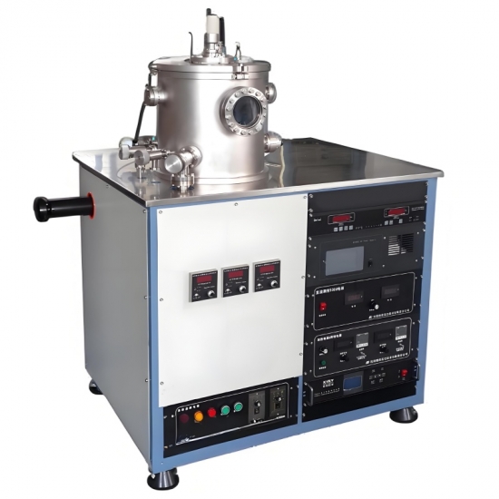
Film Deposition System
Applications
Atomic Layer Deposition is widely applied across multiple high-tech industries:
* Semiconductors: Deposition of dielectric layers, gate oxides, and high-k materials for integrated circuits and advanced memory devices.
* Optics and Photonics: Creation of anti-reflective coatings, optical filters, and multilayer mirrors with precise thickness control.
* Nanotechnology: Fabrication of nanoscale thin films, core-shell nanoparticles, and conformal coatings on complex 3D nanostructures.
* Energy Devices: Coating electrodes and protective layers in batteries, fuel cells, and photovoltaic devices.
* Biomedical Applications: Deposition of biocompatible coatings and protective layers on implants, sensors, and medical devices.
Advantages
ALD systems offer several key advantages over conventional deposition techniques:
1. Atomic-Level Precision: Enables control of film thickness and composition at the atomic scale.
2. Exceptional Conformality: Uniform coating of complex 3D structures and high-aspect-ratio substrates.
3. High Purity and Quality: Self-limiting reactions reduce contamination and defects.
4. Repeatable and Reliable: Automated cycles ensure consistent deposition across multiple runs.
5. Versatility: Capable of depositing metals, oxides, nitrides, and hybrid materials.
6. Low Thermal Stress: Enables coating of temperature-sensitive substrates due to moderate processing temperatures.
Conclusion
Atomic Layer Deposition represents a revolutionary approach to thin film fabrication, offering atomic-level control, excellent conformality, and unparalleled uniformity. ALD systems are indispensable for applications requiring high-performance coatings, including semiconductors, optics, nanotechnology, energy devices, and biomedical engineering.
With its precise process control, advanced monitoring, and flexibility in material selection, ALD technology enables researchers and manufacturers to fabricate complex multilayer structures and functional coatings with exceptional reproducibility. As demand for miniaturized, high-performance devices grows, Atomic Layer Deposition continues to play a vital role in advancing materials science, nanotechnology, and next-generation device manufacturing.


 +86 13174506016
 Louis@lithmachine.com
 +86 18559646958
 18659217588
 English ▼


