Lith Corporation, founded in 1998 by a group of material science doctor from Tsinghua University, has now become the leading manufacturer of battery lab&production equipment. Lith Corporation have production factories in shenzhen and xiamen of China.This allows for the possibility of providing high quality and low-cost precision machines for lab&production equipment,including: roller press, film coater,mixer, high-temperature furnace, glove box,and complete set of equipment for research of rechargeable battery materials. Simple to operate, low cost and commitment to our customers is our priority.
Conductive Coating: Overview, Features, Process, Applications, Advantages, and Conclusion
Conductive Coating technology refers to the process of depositing a thin layer of electrically conductive material onto a substrate, providing enhanced electrical, thermal, and surface properties. This type of coating is widely used in industries such as electronics, energy storage, sensors, aerospace, and research laboratories. Conductive coatings can be applied using various techniques, including Physical Vapor Deposition (PVD), sputtering, electroplating, and chemical vapor deposition, depending on the material and application requirements. Among these, PVD sputtering and DC/ion sputtering methods are preferred for achieving high-quality, uniform, and adherent conductive films.
Overview
A Conductive Coating system is designed to deposit metals or conductive compounds onto substrates to improve surface conductivity and enable applications such as electromagnetic shielding, sensor functionality, transparent electrodes, and SEM sample preparation. Modern conductive coating systems are capable of precise control over film thickness, uniformity, and material composition. They are widely employed in research, electronics manufacturing, and surface engineering due to their reliability, repeatability, and scalability.
Key Features of Conductive Coating Systems
High-performance conductive coating systems possess several essential features:
Vacuum Chamber Design: Ensures low contamination and high-purity deposition for sensitive substrates.
Sputtering or Deposition Source: Can include DC, RF, or magnetron sources to efficiently deposit metals, alloys, or conductive oxides.
Automated Substrate Handling: Rotating, tilting, or biasing mechanisms ensure uniform coating on complex geometries.
Power Supply Control: Stable DC or RF power sources maintain consistent plasma for precise deposition rates.
Process Monitoring and Automation: Real-time monitoring of deposition rate, thickness, and plasma parameters improves reproducibility and quality.
These features allow conductive coating systems to produce consistent, high-performance films tailored for advanced technological applications.
Conductive Coating Process
The conductive coating process typically involves several key steps:
Vacuum Preparation: The chamber is evacuated to a high vacuum to minimize contamination and oxidation.
Plasma Generation: An inert gas, such as argon, is introduced, and plasma is generated using DC, RF, or pulsed power sources.
Sputtering or Deposition: Positive ions bombard the conductive target material, ejecting atoms that condense onto the substrate to form a uniform, adherent thin film.
Optional Reactive Process: Reactive gases like oxygen or nitrogen can be introduced to produce conductive compounds, such as metal oxides or nitrides.
Film Thickness Control: Automated systems or quartz crystal microbalances monitor deposition rate and final film thickness to ensure precision.
Variations of this process, including magnetron sputtering or co-sputtering, can be employed for higher deposition efficiency, multilayer films, or alloyed coatings.
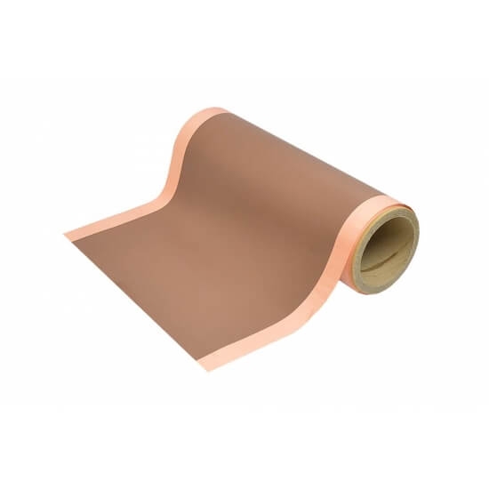
Carbon Coated Copper Foil
Applications
Conductive coatings have a broad range of industrial and research applications:
Electronics and Semiconductors: Formation of conductive traces, interconnects, electrodes, and thin-film devices.
Microscopy and Analytical Instruments: Coating non-conductive samples for SEM or AFM imaging to prevent charging effects and improve image resolution.
Energy Storage: Deposition of transparent conductive oxides and electrode materials for solar cells, batteries, and supercapacitors.
Surface Engineering: Wear-resistant, corrosion-resistant, and electromagnetic shielding coatings on metals, plastics, and ceramics.
Sensors and MEMS Devices: Enhances electrical functionality in microelectromechanical systems and sensor surfaces.
Advantages
The key advantages of conductive coating technology include:
High Conductivity: Provides efficient electrical pathways for functional devices or analytical samples.
Uniform and Dense Films: Ensures strong adhesion and smooth surface morphology.
Material Versatility: Can deposit metals, alloys, conductive oxides, and composites.
Low Substrate Heating: Enables coating on temperature-sensitive materials, such as polymers and delicate electronics.
Excellent Reproducibility and Control: Automated process parameters ensure consistent thickness, composition, and surface quality.
Enhanced Surface Properties: Improves corrosion resistance, wear resistance, and optical properties where required.
Conclusion
In conclusion, Conductive Coating technology is a versatile, precise, and indispensable tool for a wide range of industrial and research applications. By providing uniform, adherent, and high-performance conductive films, these systems enable critical functions in electronics, surface engineering, energy devices, and analytical instrumentation. With advanced process control, material versatility, and high reproducibility, conductive coating systems continue to play a pivotal role in modern technology, supporting innovations in electronics, energy, and material science.


 +86 13174506016
 Louis@lithmachine.com
 +86 18559646958
 18659217588
 English ▼


